
From high-purity molybdenum trioxide to electronic-grade molybdenum disulfide: Semiconductor applications and industrialization pathways
As silicon-based transistors shrink to the 2-nanometer node, leakage current and heat generation caused by quantum tunneling have become a physical bottleneck hindering the continued evolution of Moore's Law. Molybdenum disulfide (MoS₂), with an atomic layer thickness of only about 0.7 nanometers , is considered a key channel material candidate for breakthroughs in sub-1-nanometer processes due to its inherent immunity to short-channel effects in its ultrathin structure HYPERLINK "https://ieeexplore.ieee.org/document/11353602" \l "1" \t "_blank". However, a significant industrialization gap exists between its superior performance in the laboratory and stable manufacturing on semiconductor production lines, from "high-purity raw materials" to "wafer-level electronic-grade thin films." On this path, high-purity molybdenum trioxide ( MoO₃ ) is playing an increasingly important role—it is not the end point, but rather the starting point towards electronic-grade MoS₂ .
Introduction
As silicon-based transistors shrink to the 2-nanometer node, leakage current and heat generation caused by quantum tunneling have become a physical bottleneck hindering the continued evolution of Moore's Law. Molybdenum disulfide (MoS₂), with an atomic layer thickness of only about 0.7 nanometers , is considered a key channel material candidate for breakthroughs in sub-1-nanometer processes due to its inherent immunity to short-channel effects in its ultrathin structure HYPERLINK "https://ieeexplore.ieee.org/document/11353602" \l "1" \t "_blank". However, a significant industrialization gap exists between its superior performance in the laboratory and stable manufacturing on semiconductor production lines, from "high-purity raw materials" to "wafer-level electronic-grade thin films." On this path, high-purity molybdenum trioxide ( MoO₃ ) is playing an increasingly important role—it is not the end point, but rather the starting point towards electronic-grade MoS₂ .
I. Semiconductor Application Prospects of Electronic-Grade Molybdenum Disulfide
1. Transistor Channel: A Core Candidate in the Post-Moore's Law Era
The most fundamental value of MoS₂ in the semiconductor industry lies in its potential as a channel material for field-effect transistors (FETs). Monolayer MoS₂ has a direct bandgap of approximately 1.8 eV, and possesses both atomic-level thickness and excellent gate electrostatic control capabilities, enabling it to effectively suppress short-channel effects even at gate lengths below 10 nanometers.
In December 2025, the team led by Wang Xinran and Li Weisheng at Nanjing University developed antimony crystal epitaxial contact technology , achieving low-resistance ohmic contacts at sub-20 nm contact lengths. They successfully fabricated high-performance MoS₂ transistors for the 1 nm node , demonstrating the application potential of two-dimensional semiconductors in angstrom-era integrated circuits. Moving closer to the production line, researchers achieved, for the first time, the integration of MoS₂ stacked channel transistors on a 300 mm wafer using atomic layer deposition (ALD) combined with a "channel-back integration" scheme . They also optimized the source-drain contact—the niobium contact—achieving an ION/IOFF ratio of 10⁴ , a 28-fold improvement over the Iₒₙ of the titanium contact .
2. New types of memory: From DRAM to neuromorphic computing
The low leakage current of MoS₂ has made it a focus of attention in the memory field. In dynamic random access memory (DRAM), the capacitor-free 2T0C structure based on monolayer MoS₂ provides a new approach to solving the short-channel effect and refresh problem of traditional DRAM. In non-volatile memory, MoS₂-based ferroelectric tunnel junctions (FTJs) demonstrate the potential for polymorphic storage and in-memory computing due to their compact size, high on/off ratio, and CMOS compatibility. Furthermore, the University of Hong Kong team has further expanded the application boundaries of MoS₂ in neuromorphic computing with its analog content-addressable memory constructed using atomically thin MoS₂ flash memory and semi-metallic antimony contacts , and its deep ultraviolet programmable neuromorphic memory based on MoS₂ / β - Ga₂O₃ /multilayer graphene heterojunction (achieving an image recognition accuracy of 91.07%) .
3. Photoelectric detection and flexible electronics
The direct bandgap of MoS₂ gives it a natural advantage in photoelectric detection. A study published in 2025 demonstrated a waveguide-integrated photodetector based on a monolayer MoS₂ , achieving zero bias operation and zero dark current at a communication wavelength of 1550 nm , with a record responsivity of approximately 180 V/W-. A self-powered broadband photodetector based on a 1T/2H MoS₂ Schottky homojunction also demonstrated high-performance optical response without the need for external bias.
In the field of flexible electronics, the atomic-level thickness and mechanical flexibility of MoS₂ make it ideal for wearable and implantable devices . Flexible active arrays based on MoS₂ have been used for high-fidelity spatiotemporal monitoring of neural activity in electroencephalography (EEG) sensors, achieving high-density signal acquisition using a dual-transistor multiplexed source follower architecture. Flexible MoS₂ thin -film transistors, employing strain-engineered dual-gate structures with graphene electrodes, are also continuously pushing the performance boundaries of transparent and flexible electronic devices.
4. System-level integration: From transistors to microprocessors
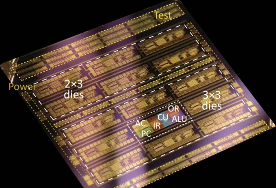
MoS₂ are no longer limited to the level of individual devices. In May 2026, Nanjing University, in collaboration with Suzhou National Laboratory and Huawei Technologies Co., Ltd., successfully developed the world's first two-dimensional semiconductor multi-bit parallel microprocessor, "Dream Start-1000," on an ultrathin MoS₂ material with a thickness of only 0.6 nanometers. This achievement increased the integration density of non-silicon new material chips by 14 times and, for the first time, realized parallel computing and on-chip register file functions on a two-dimensional platform. This milestone marks a key leap for two-dimensional semiconductors from functional verification to system-level integration.
II . Preparation of electronic-grade MoS₂ using high-purity MoO₃ as a precursor
1. Why choose the MoO₃ route ?
Purifying molybdenum concentrate to the 4N/5N level involves a complex process involving multiple acid leaching steps, hydrofluoric acid treatment, and chloride leaching, each of which may introduce new impurities or process variables. Using high-purity MoO₃ (≥99.9%) as the molybdenum source essentially moves the purity control point forward— MoO₃ , as a mature industrial product, already has a controllable low level of metallic impurities. Subsequent sulfidation reactions only need to focus on the atomic substitution of "oxygen → sulfur," significantly reducing process variables .
2. Core vulcanization process route
(1) CVD vapor phase sulfidation: the mainstream path for wafer-level thin films
Chemical vapor deposition (CVD) uses high-purity MoO₃ powder and sulfur powder as precursors, which are heated and evaporated in a tube furnace . The MoO₃ vapor reacts with sulfur vapor on the substrate surface to form MoS₂ . A key challenge of this route is suppressing the formation of MoO₃₋ₓ intermediates —these suboxides lead to the formation of MoO₂ - MoS₂ hybrid structures, contaminating the final product. Studies have shown that maintaining a certain MoO₃ evaporation atmosphere near the growth substrate while increasing the sulfur sublimation rate can significantly suppress the deposition of intermediates, thereby obtaining pure and clean large-scale MoS₂ crystals on Si/ SiO₂ substrates. MoS₂ transistors based on this route have exhibited good carrier mobility and device on/off ratios.
(2) Two-step thermal vulcanization: for wafer-level uniformity
A more suitable approach for large-scale production employs a two-step thermal process : first, the MoO₃ film is reduced to low-valence molybdenum oxide in a hydrogen atmosphere at 500°C, followed by sulfidation in a sulfur atmosphere at 1000°C to obtain a wafer-level MoS₂ thin layer . Complementing this is an ALD-assisted two-step method —first, a wafer-level, thickness-controllable MoO₃ layer is generated on the substrate surface using an atomic layer deposition system , and then the MoO₃ is sulfidated to generate MoS₂ , thus achieving precisely controllable layer number preparation of wafer-level MoS₂ . The key advantage of this approach is that the ALD deposition of MoO₃ possesses self-limiting surface saturation adsorption characteristics, ensuring the uniformity of the precursor film thickness from the source.
(3) MOCVD route: direct connection with semiconductor production lines
, developed a metal-organic chemical vapor deposition (MOCVD) route to achieve wafer-level epitaxial growth of a single-layer MoS₂ monocrystalline film on a c -plane sapphire substrate using MoO₂Cl₂ as a molybdenum precursor . The unique feature of this method is the discovery of a thickness self-stopping mechanism —even with extended growth time, the second layer hardly grows, and the film thickness remains uniform across a 2-inch scale, promising applications on 300 mm wafers. The fabricated MoS₂ transistors achieved a mobility of 66 cm²/Vs at room temperature and 749 cm²/Vs at 20 K. The temperature dependence indicates that phonon scattering is dominant, confirming the high-quality single-crystal characteristics with virtually no grain boundaries . The process compatibility of MOCVD with existing semiconductor industries makes it one of the most promising routes for the industrialization of electronic-grade MoS₂ .
3. From 3N to 4N/5N: The purity ladder still to be traversed
It is important to recognize that while the direct products of the CVD/MOCVD route using MoO₃ as a precursor typically achieve a chemical purity of 3N-4N, consistently reaching 5N (99.999%) while simultaneously meeting the stringent requirements for lattice defect density in semiconductor-grade applications still faces the following systemic challenges:
Sulfur source purity : Trace metal and carbon impurities in industrial sulfur powder may be incorporated into the MoS₂ lattice during high-temperature sulfidation . Using high-purity sulfur (such as 5N-grade sublimed sulfur) is necessary, but the cost increases significantly.
Reactor contamination : Trace contamination from the quartz tube, carrier gas (high-purity Ar /H₂ ) , and substrate processing can affect device performance even at the ppb level. This necessitates operating the entire process chain in a clean environment or employing in-situ cleaning protocols.
Defect control : Sulfur vacancies and grain boundaries, common in CVD growth, can become carrier scattering centers and leakage channels even when chemical purity meets requirements. MOCVD's self-stopping single-crystal growth mechanism has a natural advantage in defect control, but the purity and supply stability of the precursor MoO₂Cl₂ still need to be optimized .
Post-processing purification : For electronic-grade MoS₂ in powder form , the sulfidation products may still need to be purified by vacuum volatilization (taking advantage of the sublimation of MoS₂ at around 450°C) or zone melting , etc., to remove residual sulfur and volatile byproducts.
III. Summary and Outlook
electronic-grade MoS₂ in the semiconductor industry is rapidly shifting from a "promising candidate material" to an "integrable engineering material." Between 2025 and 2026, a series of milestones, including 300 mm wafer-level ALD integration , 1-nanometer node transistor demonstrations , and the world's first two-dimensional microprocessor , mark the critical point for two-dimensional semiconductors to cross from the laboratory to the production line.
In this process, high-purity MoO₃ has unique industrialization advantages as a molybdenum source : it simplifies the complexity of impurity control from "multi-step hydrometallurgy" to "purity assurance of a single precursor," and enables the direct application of thin-film deposition technologies compatible with semiconductor production lines, such as CVD, ALD, and MOCVD. However, achieving the purity leap from 3N to 5N, and comprehensively meeting the standards from "chemical purity" to "device-level crystal quality," still requires the coordinated advancement of systematic technologies such as deep purification of the sulfur source, clean control of the reaction environment, and defect engineering.
Shanghai Canal supplies high-purity molybdenum trioxide to Climax in the United States. It is produced using both wet and sublimation processes, with a purity of up to 99.99%, and is specifically designed for the semiconductor industry.
https://www.canalchem.com/products/prd-category-004/product-059.html